
2026 Global Advanced Packaging Market Exceeds $60B – Supply Chain Breakdown
The advanced packaging market has entered a new phase. In 2026, global revenue is expected to exceed $60 billion, a scale that would have seemed surprisingly high only a few years ago. What changed is not just demand, but the nature of demand itself: AI accelerators, high-bandwidth memory, chiplets, and heterogeneous integration have turned advanced packaging from a niche technology into a core growth engine for the semiconductor industry. The headline number is impressive, but the real story is the supply chain underneath it.
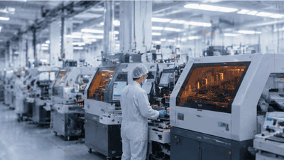
This market is no longer a simple back-end extension of wafer fabrication. It is a complex ecosystem spanning foundries, OSATs, substrate makers, interposer suppliers, equipment vendors, materials companies, and test houses. Each layer of that chain is under pressure, and each layer is now strategically important. To understand why the market can exceed $60 billion while still feeling constrained, it helps to break down the supply chain segment by segment.
Why the Market Is Growing So Fast
Advanced packaging is growing because the industry has run into the practical limits of monolithic scaling. The biggest AI chips now rely on multi-die integration, HBM stacks, and package-level bandwidth that was once unthinkable. That means the package itself is doing much more of the system’s heavy lifting.
Several forces are driving the surge:
- AI training and inference demand are increasing the number of high-end accelerators shipped each year.
- Chiplet architectures are pushing more dies into a single package, raising content per unit.
- HBM integration is becoming standard in premium AI and HPC devices, which directly lifts packaging complexity and value.
- Mobile, automotive, and networking applications are also adopting more advanced encapsulation methods, broadening the market base.
The result is a market that is growing in both volume and complexity. More packages are being built, and each package contains more value, more materials, and more process steps. That combination is why the total market can clear $60 billion even before considering the knock-on effects of capacity shortages and premium pricing.
The New Supply Chain Map

The supply chain for advanced packaging has become a layered system with many interdependencies. A simplified breakdown looks like this:
- Foundries provide advanced wafer fabrication and, in some cases, integrated packaging services.
- OSATs handle assembly, test, system-in-package integration, and increasingly advanced 2.5D and 3D packaging flows.
- Substrate and interposer suppliers deliver the high-density materials needed for routing and mechanical support.
- Equipment vendors supply bonders, aligners, temporary bond/debond tools, inspection systems, and related machinery.
- Materials companies provide mold compounds, underfill, photoresists, copper foils, dielectrics, and thermal interface materials.
- Test and metrology providers ensure the resulting multi-die packages meet performance and reliability targets.
The important thing to notice is that none of these segments stands alone anymore. A shortage in substrates can slow package output even if the foundry has wafers ready. A shortage in HBM can leave packaging lines underutilized. A lack of bonding tools or trained operators can delay yield ramp. The supply chain is now a tightly coupled system, not a sequence of isolated steps.
Foundries Take a Bigger Role
Foundries have moved far beyond wafer fabrication. In advanced packaging, they increasingly control the most critical integration steps, especially for AI and HPC products. Their role now includes:
- Providing 2.5D platforms such as silicon interposers for large AI packages.
- Supporting 3D stacking and hybrid bonding roadmaps.
- Coordinating wafer and packaging capacity for high-priority customers.
This is a major shift because the packaging stage has become a strategic differentiator. Foundries that can combine leading-edge logic with advanced packaging capacity can offer a more complete solution, and that matters when customers want speed, yield, and supply security all at once. In practice, the packaging backlog is now as important as the wafer backlog. For some customers, it is the packaging line—not the fab—that determines when a product can actually ship.
OSATs: The Flexibility Layer
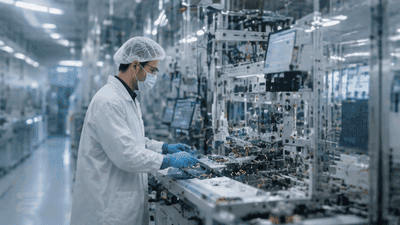
Outsourced semiconductor assembly and test providers remain central to the market, but their role has evolved. They are no longer just the place where standard packaging happens after wafers leave the fab. The leading OSATs now support advanced fan-out, chiplet assembly, HBM integration, and increasingly complex 2.5D/3D systems.
Their strengths are flexibility and scale. OSATs often serve a wide range of customers across mobile, automotive, consumer, networking, and AI. That breadth gives them a valuable perspective on how advanced packaging demand is evolving. It also means they can act as a pressure valve when foundry-run packaging lines are too full.
At the same time, OSATs face a difficult balancing act. They must invest aggressively in new equipment and process know-how without overcommitting to a single market cycle. AI demand is strong, but it is not the whole market. An OSAT that overbuilds for one type of package may find itself exposed if demand shifts. Success depends on building platforms that can serve multiple package families while still handling the most demanding AI workloads.
Substrates and Interposers: Quiet Bottlenecks
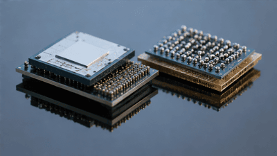
One of the most important parts of the supply chain is also one of the least visible: the substrate. For advanced packages, the substrate is not just a mechanical base. It is a high-performance electrical platform with increasingly fine routing, tighter tolerances, and more demanding material properties.
The same is true for silicon interposers and other integration layers. These components must handle dense routing between logic and memory, maintain flatness, manage thermal stress, and survive complex assembly flows. Their manufacturing requires precision that pushes the limits of existing supply chains.
Why are these materials so important? Because advanced packages often depend on:
- High-density organic substrates with multiple layers and fine line/space features.
- Silicon interposers for 2.5D AI and HPC packages.
- Glass or emerging substrate alternatives in some next-generation designs.
If substrate production lags, package output slows. If interposer supply is tight, AI accelerator shipments fall behind plan. These are not minor supporting materials; they are key enablers of the entire market. And because they require long lead times and specialized manufacturing, they are among the hardest parts of the supply chain to expand quickly.
Equipment: The Constraint Behind the Constraint
The equipment layer deserves special attention because it determines how fast the rest of the supply chain can expand. Advanced packaging requires specialized tools for:
- Die bonding and wafer bonding.
- Hybrid bonding and fine-pitch alignment.
- Temporary bonding and debonding for thin wafers.
- Inspection, metrology, and defect detection.
- Fan-out redistribution layer formation and panel-level processing.
Equipment shortages can be a hidden bottleneck. Even when a foundry or OSAT has demand, it cannot simply “spin up” a new advanced packaging line overnight. Tool procurement, installation, qualification, and operator training all take time. This means the market’s growth is partly governed by how quickly tool suppliers can deliver reliable, high-throughput machines.
Another subtle issue is tool iteration. Advanced packaging is still evolving, so customers often want tools that can support different package types, different pitches, and different substrates. That makes the equipment market both dynamic and fragmented. Vendors have to design for flexibility while still hitting the throughput and yield targets that high-volume production demands.
Materials: Small Inputs, Huge Impact
Materials often look like a supporting cast, but in advanced packaging they are central to performance and cost. Consider the number of specialized materials involved in a high-end AI package:
- Underfill and mold compounds for mechanical support.
- High-performance dielectrics and resins for redistribution layers.
- Thermal interface materials for heat extraction.
- Copper foils, barriers, and seed layers for fine interconnects.
- Adhesives and temporary bonding materials for thin-wafer handling.
Each of these materials must meet strict requirements for purity, thermal stability, moisture resistance, and compatibility with the rest of the package. A small weakness in one material can reduce yield across the entire module. That is why materials suppliers are now strategic partners, not just commodity vendors.
As package complexity rises, so does the value of material innovation. Better thermal materials can improve sustained AI performance. More stable dielectrics can support finer routing. Cleaner underfill and molding systems can improve reliability and reduce rework. In a market now worth more than $60 billion, those improvements are not marginal. They can shift the economics of whole product lines.
HBM and AI: The Demand Engine
If there is one force behind the market’s sudden rise, it is AI. Modern AI accelerators depend on huge amounts of bandwidth, which means HBM has become a critical companion to advanced packaging. Logic dies and HBM stacks are tightly coupled in packages that often require silicon interposers or equally advanced assembly platforms.
That pairing creates a multiplier effect. More AI chips means more HBM. More HBM means more complex packages. More complex packages mean more demand for substrates, interposers, bonders, and test tools. The whole ecosystem grows together.
This is one reason the market can exceed $60 billion even if other segments are growing more slowly. AI is not just adding one product category; it is pulling the entire value chain upward. A single AI package can contain more packaging value than several conventional chips combined. That changes the market math in a big way.
Regional Competition and Resilience
The supply chain breakdown is also a story about geography. Advanced packaging is concentrated in a few regions, which creates both strength and vulnerability. Some regions have deep foundry and OSAT ecosystems, while others are trying to build domestic capacity to reduce dependence and improve resilience.
This regional competition has several consequences:
- Countries and blocs are funding domestic advanced packaging infrastructure.
- Customers are diversifying suppliers to avoid single points of failure.
- Toolmakers and materials suppliers are being pulled into regional expansion efforts.
The upside is more capacity and more innovation. The downside is duplication, longer qualification cycles, and a supply chain that can be harder to coordinate globally. Still, the strategic value of advanced packaging is high enough that most major regions are willing to invest heavily in it.
Margins, Pricing, and Scarcity
A market above $60 billion is not just large; it is also increasingly valuable. Scarcity in key segments has pushed pricing higher, especially for advanced packaging services tied to AI accelerators and HBM-intensive designs. This benefits suppliers with the right capabilities and capacity, but it also makes the supply chain more expensive for customers.
There is a feedback loop here. High demand and limited capacity support premium pricing, which encourages more investment. More investment should expand capacity, but because the build-out is slow and capital-intensive, shortages can persist for years. That is why the market can be both booming and constrained at the same time.
What Comes Next
Looking forward, the supply chain will probably become even more diversified and specialized. We are likely to see:
- More hybrid bonding and 3D integration in high-end packages.
- Wider use of fan-out and panel-level packaging in mobile and consumer products.
- Greater attention to substrate innovation, including glass-based approaches in some segments.
- More regional investment in tools and materials to reduce risk and secure supply.
The market may also become more segmented by application. AI and HPC will continue to drive the highest-value packages, while automotive, mobile, and networking will shape volume growth and technology diffusion. That split means the advanced packaging supply chain must be flexible enough to serve both bleeding-edge and high-volume needs.
Conclusion
The 2026 advanced packaging market exceeding $60 billion is not just a number; it is a signal that the semiconductor industry has crossed into a new era. The package is now a major source of performance, value, and bottleneck. The supply chain behind it—foundries, OSATs, substrates, interposers, tools, materials, and test—is every bit as important as the chips themselves.
What makes this moment especially interesting is that the market’s growth is being shaped by both demand and constraint. AI, chiplets, and heterogeneous integration are creating enormous opportunity, but they are also exposing weak links in capacity and coordination. The winners in this environment will be the companies that can build, qualify, and scale the full packaging ecosystem, not just one part of it.
In that sense, advanced packaging has become more than a technology category. It is now a supply chain strategy, a manufacturing challenge, and a competitive advantage all at once.





